Printed circuit boards, or PCBs, are the backbone of most electronics, and they are found even in advanced computers. They’re found in simple digital clocks and mainframe computers, yet few people know much more than that. Whether they are making single-sided circuit boards or complex multi-layer boards, the basic manufacturing process is the same. From idea to production, here is an overview of the PCB manufacturing process.
The Design Stage
A designer will lay out the components and circuit paths using PCB design software. They will decide which components are necessary to create the final product, where they are located, and how they are all connected. The design will go through several iterations, and it is typically run through simulations to determine if it will work.
The Transition from File to Film
Once approved, the PCB design will have additional information added that is essential to the actual manufacturing of the design. For example, Altium’s stencil online generator will help the circuit designer note where solder paste and solder resist ink will be applied to the PCB during the manufacturing process. This information is needed to create paste mask layers or stencils that allow for the mass production of PCB boards. The stencils also minimize the odds that solder paste is applied to surface mount devices where it would cause them to short out.
The Manufacturing Process
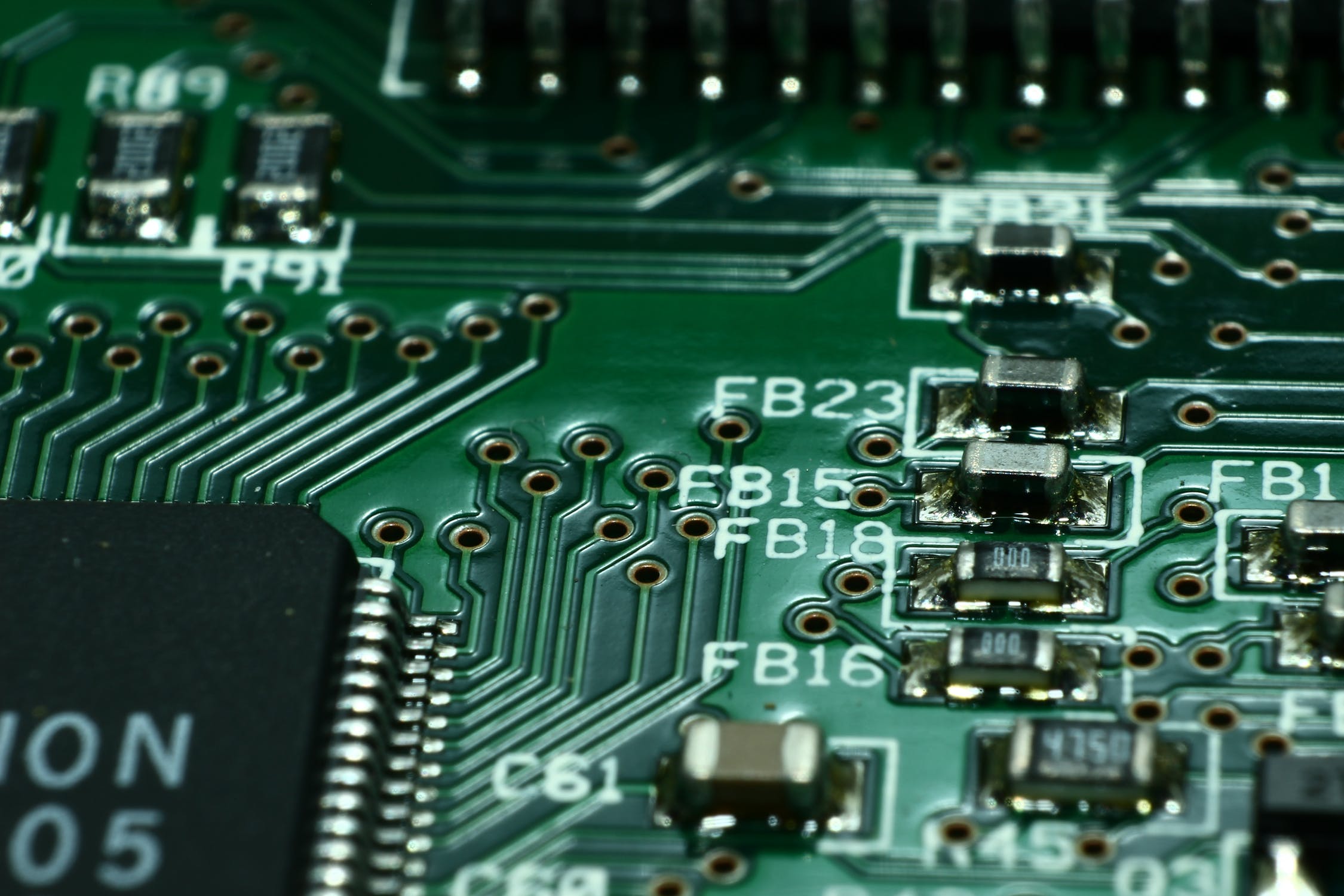
Once there is an approved design and plan for applying the solder mask, the PCB manufacturer can begin making the printed circuit boards. They’ll start by making the substrate. The substrate is made from an insulating material like fiberglass. The substrate will hold all the components in the structure.
Copper will be pre-bonded to each side of the layer and then etched per the design laid out on the printed films. A photo-sensitive film made of photo-reactive chemicals will be printed on the inner layers. It will help ensure that the actual printing of the boards is accurate. Holes in the PCB are drilled at this point; some are guide holes used to keep the layers aligned during manufacturing while they may drill other holes required by the designer at this point. Pins are inserted around this time.
Then the light-sensitive film will be exposed to ultraviolet light to harden it. This will show where the copper pathways will go. Unwanted copper is removed. The copper paths are inspected. If it passes, the board is sent on to have the outer layers of the PCB laminated to the core. More copper may be applied. Then a mechanical press is used to press the layers of the PCB together. The PCB is laminated. The laminating process applies heat and pressure while epoxy melts to help fuse the layers together.
Additional holes may be drilled at this point, and remaining copper is removed. The PCB will be plated. The board gets a thin copper layer that will seep into the drilled holes. Another layer of photoresist will be applied to the outer layer and hardened with UV light. The board is etched to create the printed circuit board connections. Then the solder mask is applied. It will be silk screened. Then it is given a final coat and cured. The final finishing is often a solderable finish to which surface mount components will be soldered.
The Quality Assessment
The PCB isn’t considered done before the circuit board is inspected and tested. A technician should perform an electrical test to ensure that it functions as intended. They check for circuit continuity and isolation tests. Continuity tests look for disconnections or open in the circuit. Isolation tests look for shorts. Shorts will be repaired before the board is sent on for final processing.
Printed circuit boards are complex pieces of engineering that at their core simply route electricity and digital signals throughout the device. This is why they share a similar manufacturing process, whether they go into simple or cutting-edge devices.